Self-assembled Ge nanostructures
Silicon-germanium (SiGe) has emerged as a promising material system for the realization of spin qubits [1]. In the past several years intense research has been devoted in studying qubits realized in quantum dots (QDs) defined in SiGe two-dimensional electron gases [2], P donors [3] and MOS devices in Si [4]. Recently, it was demonstrated that in 28Si qubit coherence times much longer than the gate-operation time can be achieved [5]. Furthermore, first steps have been made towards long-distance spin-spin coupling [6], important for implementing long distance quantum entanglement.
On the other hand, despite the predicted great properties for fast, long-lived qubits, realized with hole spins, there are much less studies addressing holes. Recently, the first hole spin qubit has been demonstrated in a nanowire field-effect transistor created in natural Si [7].
In our group we study holes confined in Ge self-assembled nanostructures. They are obtained by means of lattice-mismatched heteroepitaxial growth, i.e. when a material with a larger lattice constant (Ge) is deposited on a smaller lattice constant substrate (Si). In the so called Stranski-Krastanow growth mode, the elastic strain stored in the growing film is relaxed by the formation of three-dimensional nanostructures on top of a thin, pseudomorphic wetting layer. Hence, islands of different sizes and geometries (hut clusters, pyramids, domes) can be created [8].

Figure 1. a) SEM image of a Ge hut wire contacted with the source and the drain electrodes. b) SEM image of SiGe dome islands grown on the pre-patterned substrate.
In 2010 the first realization of single-hole transistors based on individual SiGe dome islands was reported [9]. However, in order to move towards the realization of spin qubits one has to move away from single quantum dot devices; charge sensors and double quantum dots are required. For achieving these two building blocks we took advantage of one-dimensional Ge nanowires, so called hut wires (HWs) [10]. Self-assembled hut clusters emerge after the deposition of a few monolayers of Ge. After annealing them for a few hours nanowires with lengths exceeding 1 micrometer form. A particularly interesting feature of the HWs is that they are solely oriented along [100] and [010], whereas the wire height and width remain constant below 2 and 20 nm, respectively, leading thus to very strong confinement.
A T-like structure formed by two neighboring wires allowed us to realize a charge sensor, which is electrostatically and tunnel coupled to a quantum dot [11]. By integrating the T-like structure into a radio-frequency reflectometry setup [12], we were able to demonstrate single-shot readout of a Ge quantum dot hole spin and extract a hole spin relaxation time of about 90 μs at 500 mT [13].
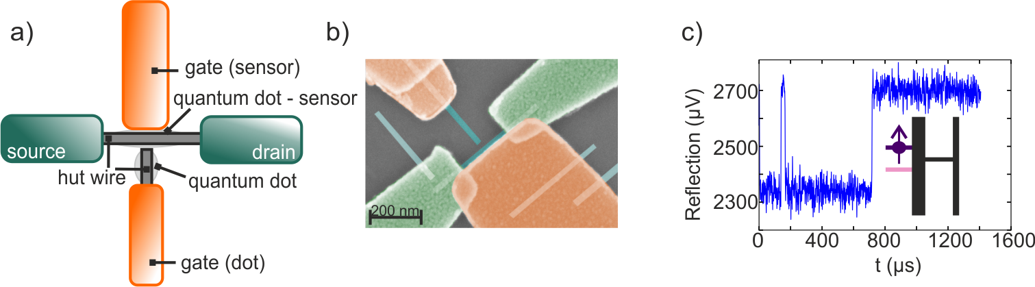
Figure 2. a) Scheme of a device used for the single-shot readout of hole spins in Ge [11]. b) SEM image of a device used for the single-shot readout of hole spins in Ge [11]. c) Example of a single-shot readout measurement for a case when a spin-up hole is loaded in the quantum dot [13].
Double quantum dot devices were realized by adding two top gates onto a HW. The strong spin orbit interaction of holes in Ge allows an all electrical control of the hole spins. Via electric dipole spin resonance coherent spin rotations of the confined hole could be demonstrated and Rabi frequencies approaching 140 MHz were obtained. Ramsey experimentes revealed dephasing times of 130 ns [14].
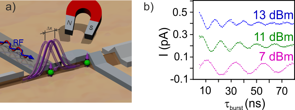
Figure 3. a) Illustration showing the principle of EDSR [14]. b) Rabi oscillations for different RF burst powers [14].
In order to realize scalable architectures, growth on pre-patterned substrates will be needed. Such growth has been successfully demonstrated for dome islands (Fig. 1b) [15]. Once the positioning of hut wires is as well controlled, the realization of more complex devices, allowing thus the coupling of multiple qubits, will become possible.
[1] F. A. Zwanenburg et al., Rev. Mod. Phys. 85, 961 (2013).
[2] N. Shaji et al., Nat. Phys. 4, 540 (2008); B. M. Maune et al., Nature 481, 344 (2012)
[3] Morello et al. Nature 467, 687 (2010)
[4] Veldhorst et al. Nature 526, 410, (2015)
[5] J. Yoneda et al. Nature Nanotech. 13, 102–106, (2018).
[6] N. Samkharadze et al. Science 25 (2018); X. Mi et al. Nature 555, 599–603, (2018).
[7] R. Maurand et al. Nature Comm. 7, 13575, (2016)
[8] J. Stangl, V. Holý, and G. Bauer, Rev. Mod. Phys. 76, 725 (2004).
[9] G. Katsaros et al. Nature Nanotech. 5, 458 (2010).
[10] Z. Z. Zhang et al. Phys. Rev. Lett. 109, 085502 (2012); H. Watzinger et al., APL Materials 2, 076102 (2014).
[11] L. Vukušić et al. Nano Lett. 17, 5706 – 5710 (2017)
[12] R. J. Schoelkopf et al. Science 280, 1238-1242 (1998)
[13] L.Vukušić et al. Nano Lett., 18, 7141–7145 (2018)
[14] H. Watzinger, J. Kukučka et al. Nature Comm. 9, 3902 (2018)
[15] Z. Zhong, G. Bauer. Appl. Phys. Lett. 1922, 84, (2004)

You must be logged in to post a comment.